This is the third part of the series. Part 1 defined AI infrastructure as the implementation layer that maps models onto hardware under a service objective. Part 2 showed how model work, context, output, and agent loops multiply demand. Part 4 treats edge intelligence as its own hardware, economics, and model-quality problem.
This part looks forward from the supply side. The prediction is simple: AI infrastructure will become more heterogeneous, and more hardware will be designed around LLM-specific bottlenecks rather than generic FLOPs.

General-purpose GPUs will remain central, but the winning system increasingly looks like a coordinated package: CPUs for orchestration, GPUs for dense math, tensor engines for narrow numerical formats, NPUs for local inference, HBM and SRAM for locality, scale-up fabrics for model parallelism, scale-out networks for cluster scheduling, and software that can place work across all of them.
The evidence falls into three constraints. Compute progress increasingly depends on narrower numerical contracts. Memory determines how much model and context can stay close to arithmetic. Communication determines whether many accelerators behave like one system.
1. Compute becomes specialized
Key insightFuture compute gains increasingly come from narrower numerical contracts and workload-specific engines, not transistor shrink alone.
Peak math is conditional
The H100 is a useful example. NVIDIA’s Hopper material highlights HBM3 bandwidth around 3 TB/s, a 50 MB L2 cache, Transformer Engine support, NVLink/NVSwitch scale-out, and low-precision tensor paths.1 These are not just “more FLOPs.” They are area, power, and system-design choices that help specific workload shapes.
The GPU timeline shows the same pattern:
| generation | headline compute direction |
|---|---|
| Tesla C870 / C1060 | CUDA-era single-precision throughput |
| K20X | higher FP32/FP64 HPC throughput |
| P100 / V100 | FP16 and Tensor Core acceleration |
| A100 / H100 | BF16, TF32, FP8, sparsity, larger memory systems |
| Blackwell / Rubin | FP4/NVFP4 and rack-scale AI systems |
Representative figures make the jump visible. Tesla C870 was advertised at 518 GFLOP/s peak single precision in 2007.2 C1060 reached 933 GFLOP/s in 2008.3 K20X reached 3.95 TFLOP/s single precision and 1.31 TFLOP/s double precision in 2012.4 P100 delivered 21.2 TFLOP/s FP16 in 2016, V100 delivered about 125-130 Tensor TFLOP/s, A100 reached 312 TFLOP/s dense FP16/BF16 Tensor Core performance, and H100 lists 1,979 TFLOP/s FP16/BF16 Tensor Core with sparsity, or half that without sparsity.5678
Blackwell continues the shift. NVIDIA’s DGX B200 system lists 144 PFLOP/s FP4 Tensor Core performance across eight Blackwell GPUs, roughly 18 PFLOP/s per GPU at the published system level, while Blackwell Ultra emphasizes 15 PFLOP/s dense NVFP4 per GPU.910 NVIDIA’s preliminary Rubin specifications list 4 PFLOP/s dense FP16/BF16 and 50 PFLOP/s NVFP4 inference compute per GPU. Vera Rubin NVL144 CPX is framed around 8 exaFLOP/s of rack-scale AI performance for massive-context inference.111213
These figures are not an apples-to-apples speedup curve. The datatype, sparsity mode, memory system, and programming model all changed. That is the important part. GPU progress came from changing the numerical contract: CUDA, SIMT execution, HBM, NVLink, tensor cores, TF32, BF16, FP8, FP4, sparsity, and compiler/runtime support made model structure visible to hardware.
Three views of GPU economics
Show normalization method and GPU price data
Peak compute, launch purchase price, and current rental price answer different questions. Keep them separate, but normalize both cost views against the same dense peak compute:
Tesla C870 predates FP16 Tensor Cores, so its FP32 peak is a legacy proxy. Every later point uses dense FP16/BF16 without sparsity or lower-precision headline modes.81411 C870 uses its standalone launch price. P100, V100, and A100 use documented DGX launch prices divided by eight GPUs. H100 and B200 use launch-window DGX-equivalent system estimates on the same per-GPU basis.151617
Show launch purchase data
| GPU | normalized compute used | launch-price basis | launch cost/GPU | USD per peak PFLOP/s |
|---|---|---|---|---|
| Tesla C870 | 0.518 TFLOP/s FP32 proxy | standalone list price | USD 1,499 | USD 2.89M |
| Tesla P100 SXM2 | 21.2 TFLOP/s FP16 | DGX-1: USD 129,000 / 8 | USD 16,125 | USD 761K |
| Tesla V100 SXM | 125 TFLOP/s Tensor | DGX-1V: USD 149,000 / 8 | USD 18,625 | USD 149K |
| A100 SXM 80GB | 312 TFLOP/s FP16/BF16 Tensor | DGX A100: USD 199,000 / 8 | USD 24,875 | USD 79.7K |
| H100 SXM 80GB | 989 TFLOP/s dense FP16/BF16 Tensor | DGX-equivalent estimate: USD 269,000 / 8 | USD 33,600 | USD 34.0K |
| B200 SXM6 | 2,250 TFLOP/s dense FP16/BF16 Tensor | DGX B200 launch-window listing: USD 515,410 / 8 | USD 64,426 | USD 28.6K |
Show current cloud rental data
For the current rental view, use one provider and one bundle size: Lambda’s eight-GPU on-demand tier. That gives a continuous currently offered series from V100 through B200 without mixing providers or commitment discounts.18
| GPU | dense compute | current USD/GPU-hour | rental USD per PFLOP-s |
|---|---|---|---|
| Tesla V100 16GB | 0.125 PFLOP/s | USD 0.79 | USD 0.00176 |
| A100 SXM 80GB | 0.312 PFLOP/s | USD 2.79 | USD 0.00248 |
| H100 SXM 80GB | 0.989 PFLOP/s | USD 3.99 | USD 0.00112 |
| B200 SXM6 | 2.250 PFLOP/s | USD 6.69 | USD 0.000826 |
These are infrastructure proxies, not chip MSRPs or workload benchmarks. Dividing a DGX price by eight allocates CPUs, memory, storage, networking, and chassis cost to each GPU; the H100 and B200 values are launch-window estimates rather than NVIDIA-published standalone prices.17 Rental prices also include the provider’s host system, operations, capacity, and margin. That is why the current rental curve can move differently from launch purchase economics: in Lambda’s current catalog, A100 costs more per theoretical unit of dense compute than V100, then H100 and B200 resume the decline. Rubin appears only in peak compute because comparable purchase and rental prices are not yet public.
Epoch AI’s broader historical work reaches the same qualitative conclusion: GPU FLOP/s per dollar doubled roughly every 2.5 years across 2006-2021, and its newer AI hardware trend page estimates AI chip performance per dollar improving by about 37% per year across 2012-2025.1920 Our World in Data republishes the same broad compute-per-dollar series as an interactive chart, adjusted for inflation.21
Peak compute
Dense FP16/BF16 TFLOP/s where available; logarithmic scale
Historical buy cost
Release-era USD per peak PFLOP/s; lower is better
Current rental cost
Lambda eight-GPU on-demand USD per PFLOP-second; lower is better
A BOM proxy shows where the dollars moved
Key insightArithmetic is only a small attributed share of accelerator manufacturing cost. H20 makes the memory tax especially visible: its 96 GB HBM subsystem likely represents well over half of module cost.
H20 accelerator module
Estimated manufacturing proxy; about USD 2.6K
B200 accelerator module
Estimated manufacturing cost share; about USD 6.4K
Rubin VR200 NVL72 rack
Analyst procurement BOM proxy; about USD 7.8M
The H20 is the most directly relevant case for inference fleets using it today. Epoch AI’s component dataset assigns roughly USD 2.59 billion of median logic, CoWoS, HBM, and auxiliary spend to H20 production in Q3-Q4 2024. Reuters reported that NVIDIA shipped approximately one million H20s in 2024, implying a rough USD 2,600 manufacturing cost per module, with a deliberately broad USD 2,100-3,100 sensitivity range.22 On this basis, HBM contributes about 57.9%, CoWoS packaging 16.6%, all logic 15.1%, and module auxiliary components 10.4%.
The important operational point is that H20 is memory-rich but compute-restricted: it carries 96 GB of HBM3 and about 4 TB/s of memory bandwidth, while its exported compute configuration is far below H100.23 Applying the same illustrative 60/15/25 logic-area allocation attributes about 9.1% of module cost to SM/ALU structures and 2.3% to on-chip SRAM. Those are manufacturing allocations, not utilization: disabled or restricted compute structures still consume die area and wafer cost. The module sold for roughly USD 12,000-15,000 in 2024, so procurement price also includes NVIDIA margin, channel margin, software value, and market conditions rather than mapping directly to BOM.24
Epoch AI estimates a B200 module at roughly USD 5,700-7,300, centered near USD 6,400. Its central component estimates are USD 2,900 for 192 GB of physically packaged HBM3E, USD 1,100 for CoWoS-L packaging, USD 900 for two logic dies, USD 1,000 for packaging yield loss, and USD 480 for module power delivery, PCB, assembly, and testing.25 Shipping B200 specifications expose 180 GB as usable GPU memory; the BOM model prices the physical HBM capacity. The component midpoints sum to USD 6,380, close to the model’s rounded headline.
The die itself is not sold as separate ALU and SRAM line items. The left chart therefore applies a deliberately round area allocation to the USD 900 logic-die cost. Under the 60/15/25 midpoint, arithmetic and SM structures contribute about 8.5% of module manufacturing cost, on-chip SRAM about 2.1%, and other die logic about 3.5%. A broad 50-70% compute and 10-20% SRAM sensitivity moves those first two shares only to roughly 7-10% and 1.4-2.8%. The exact floorplan is undisclosed; the architectural anchor is that B200 exposes about 126 MB of shared L2 plus large per-SM register and local-memory structures.26
At rack scale, a 2026 Morgan Stanley estimate puts VR200 NVL72 at USD 7.80 million: USD 3.96 million for 72 Rubin GPUs, USD 2.00 million for memory, USD 720,000 for NVLink Switch and other networking chips, USD 180,000 for Vera CPUs, and the remainder for cooling, power, boards, substrates, passives, assembly, and other platform content.27 That gives the quick rack-level ratio: GPU packages 50.7%, memory 25.7%, communication 9.2%, CPUs 2.3%, and platform/power/cooling 12.1%. NVIDIA’s public topology confirms the physical reason communication has its own bill: an NVL72 domain contains 18 compute trays, nine NVLink Switch trays, and 72 GPUs.28
Show the BOM proxy and sensitivity assumptions
| view | attributed category | USD proxy | share | confidence |
|---|---|---|---|---|
| H20 module | SM / ALU / tensor compute | USD 236 | 9.1% | low; 60% of logic-cost assumption |
| H20 module | on-chip SRAM | USD 59 | 2.3% | low; 15% of logic-cost assumption |
| H20 module | other die logic and I/O | USD 98 | 3.8% | low; residual 25% of logic cost |
| H20 module | 96 GB HBM3 | USD 1,505 | 57.9% | medium; shipment-normalized component model |
| H20 module | CoWoS-S packaging | USD 432 | 16.6% | medium; shipment-normalized component model |
| H20 module | module auxiliary components | USD 269 | 10.4% | medium; shipment-normalized component model |
| B200 module | SM / ALU / tensor compute | USD 540 | 8.5% | low; 60% of logic-die cost assumption |
| B200 module | on-chip SRAM | USD 135 | 2.1% | low; 15% of logic-die cost assumption |
| B200 module | other die logic and I/O | USD 225 | 3.5% | low; residual 25% of logic-die cost |
| B200 module | 192 GB physical HBM3E; 180 GB exposed | USD 2,900 | 45.5% | modeled component estimate |
| B200 module | CoWoS-L plus package yield loss | USD 2,100 | 32.9% | modeled component estimate |
| B200 module | module auxiliary components | USD 480 | 7.5% | modeled component estimate |
| Rubin VR200 NVL72 | 72 GPU packages | USD 3,960,000 | 50.7% | analyst procurement estimate |
| Rubin VR200 NVL72 | memory: HBM4, CPU memory, and storage | USD 2,001,600 | 25.7% | analyst aggregate; not HBM-only |
| Rubin VR200 NVL72 | NVLink Switch plus other networking chips | USD 720,000 | 9.2% | sum of two analyst line items |
| Rubin VR200 NVL72 | Vera CPUs | USD 180,000 | 2.3% | analyst procurement estimate |
| Rubin VR200 NVL72 | power and cooling | USD 148,080 | 1.9% | sum of two analyst line items |
| Rubin VR200 NVL72 | boards, substrate, passives, assembly, and other | USD 793,468 | 10.2% | residual from reported total |
These are neither NVIDIA’s internal costs nor retail margins. The H20 estimate additionally mixes a component-production timeline with a shipment denominator, so treat its USD values as an order-of-magnitude allocation rather than accounting data. The module views exclude R&D, software, networking, and server infrastructure. The Rubin view is a forward-looking customer procurement estimate reported from a circulating analyst table; specifications, memory contracts, and final system pricing can move materially.
ALU manufacturing: narrow math buys more lanes
The ALU-level version of the story is simpler. Arithmetic got cheaper because accelerators stopped treating every operation as a wide general-purpose floating-point operation.
Show the FP16 ALU area-cost model
A lower-bound manufacturing proxy is:
Using Horowitz’s 45nm operation-area table and a 45nm 300mm wafer cost of about USD 2,000, the raw area-cost difference is already large before considering power, routing, register files, schedulers, or tensor-core reuse.293031
Show the 45nm operation-area baseline
| operation at 45nm | area | units per mm2 | raw cost per 1M units | area advantage |
|---|---|---|---|---|
| 16-bit FP add | 1,360 um2 | 735 | USD 38 | 3.1x vs FP32 add |
| 32-bit FP add | 4,184 um2 | 239 | USD 118 | baseline |
| 16-bit FP multiply | 1,640 um2 | 610 | USD 46 | 4.7x vs FP32 multiply |
| 32-bit FP multiply | 7,700 um2 | 130 | USD 218 | baseline |
This is the silicon reason lower-precision tensor paths can improve compute per dollar. If a workload tolerates FP16, BF16, FP8, FP4, sparsity, or structured matrix engines, the chip can spend the same die area on many more arithmetic lanes. The catch is that those lanes only become useful when the model, compiler, kernels, and memory system keep them fed.
For a rough 20-year shrinkage estimate, take the 45nm 16-bit FP add plus 16-bit FP multiply area as the baseline:
Then scale that logical datapath by public logic-density estimates. This is not a real vendor tensor-core layout. It is a normalized “same logic, denser process” estimate. The density anchors use 28/16/7nm TSMC comparisons, 5nm process-node density data, 3nm process-node density data, and next-node N2 / 18A estimates. Wafer prices reuse the same public wafer-price anchors used above; the next-node row uses a USD 30,000 wafer proxy from public 2nm pricing reports.32333435363738
N+1, N+2, and N+3 are SMIC, not TSMC, process names. They form a separate 7nm-class branch confirmed through product teardowns. Public N+1 density is not sufficiently documented for this model. For N+2, I infer about 92.9 MTr/mm2 from SemiAnalysis measurements showing N+3’s cell height and contacted-gate pitch each shrinking 9.5% from N+2. N+3 itself measures 113.4 MTr/mm2.3940
Show the process-node ALU model
| node | era | logic-density reference | estimated FP16 mul+add area | area shrink vs 45nm | units per mm2 | raw cost per 1M units |
|---|---|---|---|---|---|---|
| 45nm | 2007 | 6.25 MTr/mm2 baseline | 3,000 um2 | 1.0x | 333 | USD 85 |
| 28nm | 2010 | 15.3 MTr/mm2 | 1,225 um2 | 2.4x | 816 | USD 52 |
| 16nm | 2015 | 28.9 MTr/mm2 | 649 um2 | 4.6x | 1,541 | USD 37 |
| 7nm | 2018 | 91.2 MTr/mm2 | 206 um2 | 14.6x | 4,864 | USD 27 |
| 5nm | 2020 | 138.2 MTr/mm2 | 136 um2 | 22.1x | 7,371 | USD 33 |
| SMIC N+1, 7nm-class | 2021-2022 | teardown confirmed; density not used | not modeled | not modeled | not modeled | wafer price not public |
| SMIC N+2, 7nm-class | 2023 | about 92.9 MTr/mm2, inferred | 202 um2 | 14.9x | 4,955 | wafer price not public |
| 3nm | 2024 | 216 MTr/mm2 | 87 um2 | 34.6x | 11,520 | USD 24 |
| SMIC N+3, 7nm-class | 2025 | 113.4 MTr/mm2, teardown | 165 um2 | 18.1x | 6,048 | wafer price not public |
| N2 estimate | 2026 | 313 MTr/mm2 | 60 um2 | 50.1x | 16,693 | USD 25 |
| 18A estimate | 2026 | 238 MTr/mm2 | 79 um2 | 38.1x | 12,693 | USD 33 |
| Huawei LogicFolding roadmap | 2026 onward | 3D/package-footprint density; not a node | not comparable | not comparable | not comparable | not modeled |
The area trend is the important signal: a 16-bit floating-point multiply-plus-add datapath that is about 3,000 um2 at 45nm becomes an order of magnitude smaller by 7nm, roughly 35x smaller by 3nm, and about 50x smaller at an N2-style next node under a pure logic-density scaling model. SMIC’s N+1 to N+3 branch shows how DUV multi-patterning and design-technology co-optimization can keep improving a 7nm-class platform, but SemiAnalysis finds that N+3 pays for its TSMC N6-class density in process complexity, efficiency, and control.40
Huawei LogicFolding is a different scaling axis. Huawei describes it as shortening critical-path wiring, increasing density, and reaching its first commercial Kirin implementation in fall 2026; SemiAnalysis characterizes the approach as stacking active logic and recovering density through advanced packaging.4140 It should not be converted into a smaller planar ALU area: package-footprint density can rise by stacking active layers even when each underlying die remains on a less-dense process.
The raw wafer-cost proxy falls less smoothly because advanced wafer prices rise sharply. N2 can fit more arithmetic, but a USD 30,000 wafer can erase much of the dollar-per-ALU gain versus 3nm. Real ALUs also need registers, operand routing, control, clocking, SRAM, verification margin, and yield. Tensor cores improve the economics further by amortizing control and data movement across matrix tiles instead of treating every multiply-add as an isolated scalar unit.
Estimated raw FP16 ALU dollar cost
USD per one million multiply-plus-add datapaths; logarithmic scale
2. Memory sets the working set
Key insightModel and context capacity are constrained by where bytes live, how quickly they move, and how much each level of the memory hierarchy costs.
Memory and manufacturing show the same pattern. Compute can keep rising, but every token also needs bytes close to the math unit. The difficult part is that each level of memory optimizes a different constraint: on-chip SRAM is fast but area-expensive, HBM is bandwidth-rich but package-expensive, commodity DRAM is capacity-rich but far away, and advanced wafers are no longer getting cheap fast enough to hide the tradeoff.
Show SRAM, HBM, DRAM, and wafer methodology
On-chip SRAM: fast bytes are area-limited
For on-chip SRAM, there is no public spot price per MB. A useful lower-bound proxy is:
This ignores periphery, redundancy, yield, cache tags, routing, and design cost, so it is not a product cost. It is still useful because it shows why cache capacity is no longer free. TSMC reported a 0.127 um2 28nm 6T SRAM cell in 2009; public 5nm and 2nm SRAM reports put high-density bitcells around 0.021 um2; CSET estimated 7nm and 5nm wafer sale prices at USD 9,346 and USD 16,988 respectively; public 2026 wafer-price roundups put TSMC 3nm around USD 19,500.4243443637
Show the SRAM area-cost proxy
| node | SRAM bitcell | wafer price used | raw MB area | raw SRAM cost proxy |
|---|---|---|---|---|
| 28nm | 0.127 um2 | USD 3,000 | 1.065 mm2/MB | USD 0.045/MB |
| 7nm | 0.027 um2 | USD 9,346 | 0.226 mm2/MB | USD 0.030/MB |
| 5nm | 0.021 um2 | USD 16,988 | 0.176 mm2/MB | USD 0.042/MB |
| 3nm / 2nm-class | 0.021 um2 | USD 19,500 | 0.176 mm2/MB | USD 0.049/MB |
The punchline is not that SRAM got worse in absolute density. It got much denser. The punchline is that after 7nm, bitcell shrink is small while wafer cost keeps rising. That means larger on-chip caches require more deliberate architectural justification: more L2, more shared memory, tensor memory, larger register files, and better reuse have to earn their silicon area.
NVIDIA GPU caches show the architectural response. P100 had about 4 MB of L2, V100 6 MB, A100 40 MB, H100 50 MB, and public B200 analysis reports about 126 MB of total L2.7145 More on-chip SRAM is being used because going to HBM is expensive in energy and latency, but the amount is still tiny compared with model state and KV cache.
Off-chip memory: capacity and bandwidth diverge
Off-chip memory has split into two worlds. Commodity DRAM remains the capacity workhorse, but its price-per-GB improvement slowed sharply after 2010. Stanford DAM’s compiled memory-price dataset shows cheapest DRAM falling from about USD 185/GB in 2005 to USD 12.2/GB in 2010, then only to USD 3.0/GB by 2020 and about USD 3.45/GB in July 2026.46 HBM moves in the other direction: it is not cheap capacity, it is purchased bandwidth close to the accelerator. Rambus summarizes HBM’s speed evolution from 128 GB/s per HBM device to 2.048 TB/s for HBM4, while Stanford DAM’s modeled HBM data puts HBM2e around USD 6/GB and HBM3e peak around USD 18/GB.4746
Vera Rubin makes the next step concrete. NVIDIA’s preliminary specification assigns each Rubin GPU 288 GB of HBM4 with 22 TB/s of memory bandwidth. That is 1.6x B200’s 180 GB capacity and about 2.9x its 7.7 TB/s bandwidth. At NVL72 scale, 72 Rubin GPUs aggregate to 20.7 TB of HBM4 and 1,580 TB/s of memory bandwidth.11
Show off-chip capacity and bandwidth anchors
| off-chip memory trend | representative anchors |
|---|---|
| GPU HBM generation | P100/V100: HBM2; A100 40GB: HBM2; A100 80GB: HBM2e; H100: HBM3; B200: HBM3e; Rubin: HBM456711411 |
| GPU HBM capacity | P100: 16 GB; V100: 16 GB; A100: 40 GB; H100: 80 GB; B200: 180 GB; Rubin: 288 GB56711411 |
| GPU HBM bandwidth | P100: 720 GB/s; V100: 900 GB/s; A100: 1,555 GB/s; H100: over 3 TB/s; B200: 7.7 TB/s; Rubin: 22 TB/s56711411 |
| Vera Rubin NVL72 aggregate | 20.7 TB HBM4 capacity and 1,580 TB/s memory bandwidth across 72 Rubin GPUs11 |
| commodity DRAM price/capacity | about USD 185/GB in 2005, USD 12.2/GB in 2010, USD 3.0/GB in 2020, and USD 3.45/GB in July 202646 |
| HBM price/capacity | HBM2e around USD 6/GB, HBM3 around USD 9/GB, HBM3e peak around USD 18/GB, HBM4 projected around USD 16.5/GB46 |
| HBM price/bandwidth | HBM2e around USD 209 per TB/s, HBM3 around USD 264 per TB/s, HBM3e peak around USD 352 per TB/s, HBM4 projected around USD 297 per TB/s46 |
Manufacturing: wafer cost pushes back
The manufacturing layer is the shared denominator under both compute and SRAM. If each wafer gets more expensive, every large die, cache expansion, interposer choice, and yield loss has a higher dollar impact.
Show advanced wafer-price anchors
| process node | approximate era | wafer price anchor | why it matters |
|---|---|---|---|
| 28nm | 2010 | USD 3,000 | cheap enough that SRAM scaling still translated into lower raw MB cost |
| 7nm | 2018 | USD 9,346 | density improved, but wafer price more than tripled |
| 5nm | 2020 | USD 16,988 | raw SRAM cost proxy rose again despite smaller cells |
| 3nm | 2024 | USD 19,500 | wafer price keeps rising while SRAM bitcell shrink slows |
On-chip SRAM cost proxy
Raw bitcell USD/MB lower bound
Commodity DRAM price
Cheapest listed USD/GB; logarithmic scale
HBM bandwidth price
Modeled USD per TB/s
Advanced wafer price
Foundry sale price per 300 mm wafer; logarithmic scale
3. Communication becomes topology
Key insightOnce a model outgrows one accelerator, interconnect topology becomes part of the computer and part of model performance.
The next bottleneck appears when one accelerator is not enough. Scaling out turns compute into a distributed system problem: GPUs must exchange gradients, activations, KV cache state, expert routes, pipeline bubbles, and scheduling metadata. A useful first-order model is the latency-bandwidth model:
Here alpha is the per-message latency cost and B_effective is achieved communication bandwidth after topology, protocol, contention, and collective implementation overhead. That term matters because modern training and inference are full of collectives:
Show parallelism and scale-up bandwidth anchors
Show communication pressure by parallelism pattern
| parallelism pattern | communication pressure |
|---|---|
| data parallel | gradient all-reduce or reduce-scatter / all-gather |
| tensor parallel | activation all-reduce and all-gather inside layers |
| pipeline parallel | boundary activations and pipeline bubbles |
| expert parallel / MoE | token dispatch and all-to-all routing |
| disaggregated serving | KV cache movement, prefill/decode handoff, remote memory access |
Interconnect bandwidth is improving aggressively because this tax is now first-order. NVIDIA lists NVLink bandwidth per GPU rising from 900 GB/s on Hopper to 1.8 TB/s on Blackwell and 3.6 TB/s on Rubin; its NVLink Switch table lists NVL72 aggregate bandwidth rising from 130 TB/s on Blackwell to 260 TB/s on Rubin.48 NVIDIA’s HGX Rubin page makes the same point at the system level: higher token throughput is tied not only to more NVFP4 compute, but also to more HBM bandwidth and more NVLink Switch bandwidth.49
Show Hopper, Blackwell, and Rubin scale-up anchors
| system generation | interconnect anchor | why it matters |
|---|---|---|
| Hopper | 900 GB/s NVLink per GPU | scale-up communication becomes part of model throughput |
| Blackwell | 1.8 TB/s NVLink per GPU; 130 TB/s NVL72 aggregate | larger rack-scale GPU domains for model parallelism |
| Rubin | 3.6 TB/s NVLink per GPU; 260 TB/s NVL72 aggregate | communication bandwidth has to scale with MoE, long context, and agentic inference |
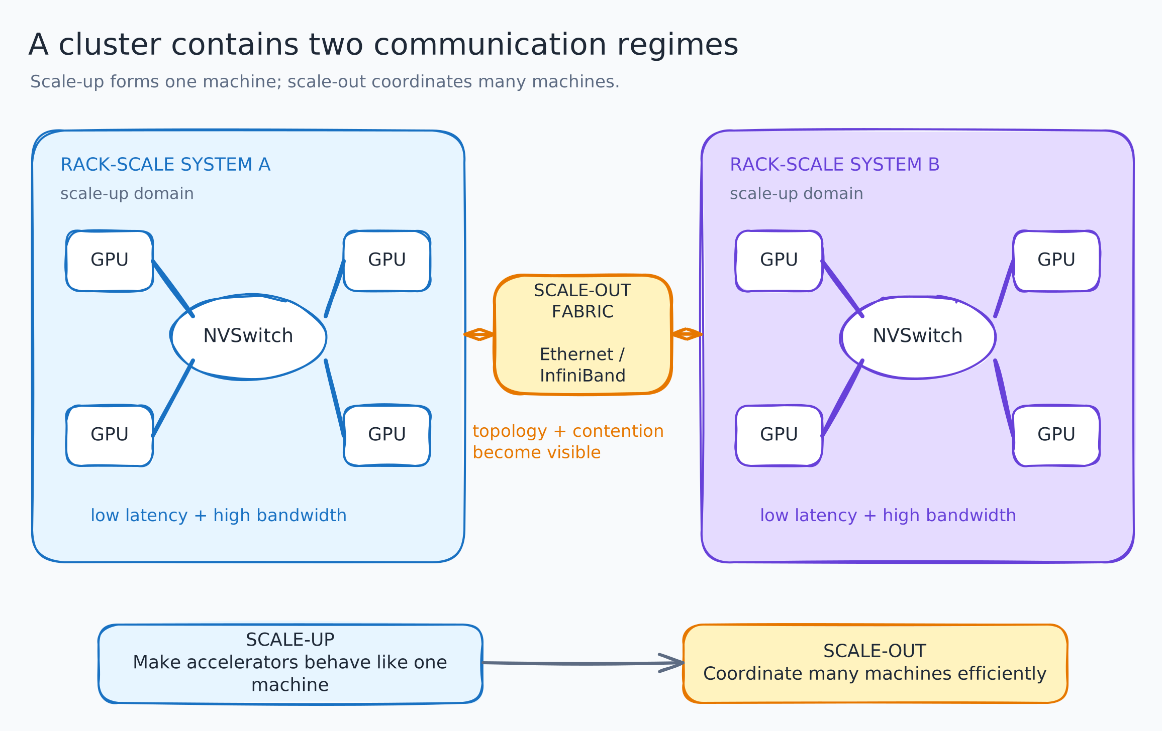
There are two different network curves hiding behind the same word “interconnect”:
- Scale-up is the tightly coupled GPU domain inside a box or rack. NVLink / NVSwitch bandwidth is not sold like a generic switch port; it is bundled into GPU systems, board design, power delivery, and thermal design. The useful public metric is bandwidth per GPU or per rack-scale domain.
- Scale-out is the cluster fabric across nodes and racks. Ethernet and InfiniBand have visible port speeds, switch radix, optics, cables, NICs, and sometimes observable street prices. This is where a rough dollar-per-Gb/s proxy is possible.
The speed curve is steep. InfiniBand moved from 4x QDR at 32 Gb/s in the late 2000s, to EDR 100 Gb/s, HDR 200 Gb/s, NDR 400 Gb/s, and XDR 800 Gb/s. Ethernet followed the same broad shape: 40/100GbE was standardized in 2010, 200/400GbE in 2017, and 800GbE in 2024.50515253 NVIDIA’s current Quantum-X800 documentation lists 72-port and 144-port XDR systems at 800 Gb/s per port, up to 115.2 Tb/s of maximum throughput for the 4U system.54
Show scale-out price methodology and switch data
For a dollar-per-speed proxy, use switch chassis price divided by front-panel bandwidth. This is not total cluster networking cost. It excludes optics, cables, NICs, support contracts, power, rack layout, and topology oversubscription. It is still useful because it shows the direction of the switching layer itself. The anchors below combine a legacy Cisco 10GbE price-list snapshot, public Mellanox / NVIDIA InfiniBand switch listings, and current SN5610 800GbE listing/spec data.55565758
Show scale-out switch price anchors
| scale-out switch proxy | approximate era | ports x port speed | public price anchor | switch dollars per Gb/s |
|---|---|---|---|---|
| Cisco Nexus 5020 10GbE | 2008 | 40 x 10 Gb/s | USD 28,770 list-price snapshot | USD 72/Gb/s |
| Mellanox SB7800 EDR | 2015 | 36 x 100 Gb/s | USD 10,259 channel listing | USD 2.85/Gb/s |
| Mellanox QM8700 HDR | 2018 | 40 x 200 Gb/s | USD 18,740 channel listing | USD 2.34/Gb/s |
| NVIDIA QM9700 NDR | 2022 | 64 x 400 Gb/s | USD 32,870 channel listing | USD 1.28/Gb/s |
| NVIDIA SN5610 800GbE | 2026 | 64 x 800 Gb/s | USD 51,999 channel listing | USD 1.02/Gb/s |
Scale-out port speed
Front-panel Gb/s; logarithmic scale
Switch cost per bandwidth
Chassis-only USD/Gb/s proxy; logarithmic scale
The punchline is subtle: network silicon has delivered a large cost-per-bit improvement, but AI clusters keep spending the savings. Higher port speed enables larger all-reduce domains, more tensor-parallel shards, more MoE all-to-all traffic, and more disaggregated serving. The value of better AI infrastructure is therefore not just “buy faster switches.” It is reducing bytes moved, placing bytes closer to compute, overlapping collectives with kernels, and choosing parallelism plans that turn expensive network bandwidth into useful tokens.
This is why “chips are slowing down” is not only a FLOP story. It is a locality and communication story. When model weights, activations, KV cache, and tool-use context grow, the system pays for bytes in several currencies: SRAM area, HBM dollars, HBM bandwidth, interconnect bandwidth, synchronization time, package complexity, wafer cost, and energy. Good AI infrastructure wins by spending fewer bytes, reusing them closer to compute, and making expensive memory and network bandwidth do useful work more often.
Edge becomes a separate placement frontier
Key insightEdge systems must optimize useful local intelligence within a product-level memory, bandwidth, thermal, power, and price envelope.
Edge hardware changes the accounting unit. A phone, AI PC, or robotics box is bounded by shared memory, bandwidth, thermals, battery life, and a product-level price rather than by rack power and HBM alone. Peak TOPS is useful, but it does not tell us how large a model fits, how quickly its weights can be streamed during decoding, or how much benchmark quality survives quantization.
Part 4 follows this edge intelligence envelope directly: how mobile, AI PC, and AI-box hardware evolved; how their product-level dollars per advertised performance changed; how edge-fit language models improved; and what those trends imply for local agents.
Prediction: heterogeneity becomes the default
Key insightThe future AI system is a coordinated heterogeneous package whose software places each workload on the right compute, memory, and communication resource.
The accounting unit connects the evidence:
token cost ~= math + memory movement + communication + scheduling + retries
The next AI infra frontier is not simply a larger cluster. It is a tighter control loop between algorithms, model architecture, serving systems, kernels, compilers, memory hierarchy, interconnect, edge devices, and chips.
The practical direction is heterogeneous and increasingly LLM-specific:
- More dedicated tensor formats and matrix engines, because narrow numerical contracts buy more useful math per watt and per dollar.
- More memory-aware architectures, because context, KV cache, retrieval, and multimodal state make bytes as important as FLOPs.
- More rack-scale and cluster-scale co-design, because scale-up and scale-out communication now shape model design.
- More edge/cloud partitioning, because not every inference should cross the network and not every local device can host the whole model.
- More compiler/runtime responsibility, because specialized hardware only matters when the software stack can expose locality, regularity, and parallelism.
The teams that win will not only have better models or better hardware. They will have better translation between the two: less work per useful result, better placement for every stage, and higher utilization of every expensive byte and arithmetic lane.
References
-
NVIDIA, NVIDIA Tesla: GPU Compute Technical Brief, 2007. ↩
-
NVIDIA, Tesla C1060 Computing Processor Board, 2008. ↩
-
NVIDIA Newsroom, NVIDIA Unveils World’s Fastest, Most Efficient Accelerators, 2012. ↩
-
NVIDIA, Pascal Architecture Whitepaper, 2016. ↩ ↩2 ↩3 ↩4
-
NVIDIA, Tesla V100 GPU Architecture, 2017. ↩ ↩2 ↩3 ↩4
-
NVIDIA, A100 Tensor Core GPU Architecture, 2020. ↩ ↩2 ↩3 ↩4 ↩5
-
NVIDIA, H100 Tensor Core GPU, accessed 2026-07-02. ↩ ↩2
-
NVIDIA Developer Blog, Inside NVIDIA Blackwell Ultra, 2026. ↩
-
NVIDIA, Vera Rubin NVL72, preliminary specifications accessed 2026-07-26. ↩ ↩2 ↩3 ↩4 ↩5 ↩6 ↩7
-
NVIDIA Newsroom, NVIDIA Kicks Off the Next Generation of AI With Rubin, 2026. ↩
-
NVIDIA Newsroom, NVIDIA Unveils Rubin CPX, 2025. ↩
-
Lenovo Press, ThinkSystem NVIDIA HGX B200 180GB 1000W GPU, accessed 2026-07-04. ↩ ↩2 ↩3 ↩4
-
Michael Feldman, NVIDIA Takes Direct Aim at High Performance Computing, HPCwire, 2007. ↩
-
NVIDIA, NVIDIA DGX-1, listing USD 129,000 for the eight-P100 system and USD 149,000 for the eight-V100 system. ↩
-
CCIR Research, Rent and MSRP: Five Generations of Posted Prices, 2026. The dataset derives per-GPU launch-window prices from eight-GPU system prices and grades the H100 and B200 estimates as vendor-adjacent rather than official standalone MSRP. ↩ ↩2
-
Lambda, GPU Instances, eight-GPU on-demand price per GPU-hour, accessed 2026-07-26. ↩
-
Jaime Sevilla and Pablo Villalobos, Trends in GPU Price-Performance, Epoch AI, 2022. ↩
-
Epoch AI, Trends in Artificial Intelligence: AI Hardware, accessed 2026-07-02. ↩
-
Our World in Data, GPU computational performance per dollar, accessed 2026-07-02. ↩
-
Epoch AI, AI Chip Components dataset and methodology, accessed 2026-08-09. The median H20 rows for Q3 and Q4 2024 sum to approximately USD 392 million logic, USD 431 million CoWoS, USD 1.500 billion HBM, and USD 268 million auxiliary spend. Epoch AI’s AI Chip Sales methodology cites approximately one million H20 shipments in 2024. Dividing component spend by shipments gives the article’s USD 2.6K module proxy; the production and shipment periods are not perfectly matched. ↩
-
NVIDIA documentation identifies the H20 SXM5 as a 96 GB Hopper GPU. Contemporary H20 product reporting lists 96 GB of HBM3, 4.0 TB/s of memory bandwidth, and 296 FP8 TFLOP/s. ↩
-
Yelin Mo and Brenda Goh, Reuters, “Nvidia’s new China-focused AI chip set to be sold at similar price to Huawei product”, 2024. NVIDIA distributor pricing was reported at USD 12,000-15,000 per card; later pricing varied with demand and export restrictions. ↩
-
Venkat Somala, Epoch AI, “NVIDIA’s B200 costs around USD 6,400 to produce, with memory accounting for half”, 2025. The model uses public reporting, analyst estimates, company disclosures, and Monte Carlo ranges; it estimates variable manufacturing cost rather than server price or NVIDIA’s full cost structure. ↩
-
Cornell Virtual Workshop, “GPU Memory Levels”, accessed 2026-08-09, summarizing B200’s 126 MB L2, 256 KB register file per SM, and 256 KB unified L1/shared memory per SM. The article’s cost allocation is an explicit proxy, not Cornell’s estimate. ↩
-
Anton Shilov, Tom’s Hardware, “Nvidia’s memory costs soar 485%, latest AI systems now cost USD 7.8 million to build”, 2026; full line-item transcription of the circulated Morgan Stanley table, 2026. This is a forward-looking analyst procurement estimate, not a public NVIDIA BOM or independently verified teardown. ↩
-
NVIDIA, “Understanding Your Grace-Blackwell Systems”, documenting the NVL72 reference configuration with 18 compute trays, nine NVLink Switch trays, and 72 GPUs. Rubin pricing is not inferred from this source; it is used only as the rack-topology anchor. ↩
-
Mark Horowitz, Computing’s Energy Problem, ISSCC 2014. ↩
-
Ting-Yu Yeh, Accelerator Architectures for Machine Learning, lecture slides citing Horowitz ISSCC 2014 operation energy and area data, accessed 2026-07-04. ↩
-
Tim Johnson, CMOS Cost, MSOE EE 4980 notes, accessed 2026-07-04. ↩
-
Team VLSI, TSMC 7nm, 16nm and 28nm Technology node comparisons, 2021. ↩
-
Wikipedia, 5 nm process, accessed 2026-07-04. ↩
-
Wikipedia, 3 nm process, accessed 2026-07-04. ↩
-
Anton Shilov, Intel’s 18A and TSMC’s N2 process nodes compared, Tom’s Hardware, 2025. ↩
-
Center for Security and Emerging Technology, Analysts believe that a single TSMC 5nm wafer costs USD 17,000, 2020. ↩ ↩2
-
Silicon Analysts, Semiconductor Wafer Pricing by Process Node, accessed 2026-07-04. ↩ ↩2
-
Astute Group, TSMC’s 2nm Wafer Price Hits USD 30,000 Amid Monopoly Concerns, 2025. ↩
-
TechInsights, Confirming SMIC N+2 7nm in Huawei Mate 60 Pro, documenting N+1 in 2022 and the commercial N+2 generation in 2023. ↩
-
SemiAnalysis STEEL Team et al., Is SMIC N+3’s Metal Pitch Smaller than Intel 18A’s?, 2026. ↩ ↩2 ↩3
-
Huawei, Huawei Presents the Tau Scaling Law, 2026. ↩
-
Mark LaPedus, TSMC devises SRAM cell at 28-nm, EE Times, 2009. ↩
-
SemiWiki, TSMC’s 5nm 0.021um2 SRAM Cell Using EUV and High Mobility Channel with Write Assist at ISSCC2020, 2020. ↩
-
TSMC Research, Memory publications, accessed 2026-07-04. ↩
-
Chips and Cheese, Nvidia’s B200: Keeping the CUDA Juggernaut Rolling, 2025. ↩
-
David Shim, Stanford DAM, Memory Prices, accessed 2026-07-04. ↩ ↩2 ↩3 ↩4 ↩5
-
Rambus, High Bandwidth Memory: Everything You Need to Know, updated 2026. ↩
-
NVIDIA, NVLink and NVLink Switch, accessed 2026-07-04. ↩
-
NVIDIA, HGX Platform, accessed 2026-07-04. ↩
-
Wikipedia, InfiniBand performance table, accessed 2026-07-04. ↩
-
Wikipedia, 100 Gigabit Ethernet, accessed 2026-07-04. ↩
-
Ethernet Alliance, IEEE 802.3 Standards Activities, 2018. ↩
-
IEEE Standards Association, Ethernet’s Next Bar is Now - 800 Gb/s!, 2024. ↩
-
NVIDIA Networking Docs, NVIDIA Q32xx and Q34xx XDR 800Gb/s InfiniBand Switch Systems, accessed 2026-07-04. ↩
-
Finnegan Software, Cisco price list snapshot, accessed 2026-07-04. ↩
-
Router-Switch.com, NVIDIA Mellanox switches price list, accessed 2026-07-04. ↩
-
NADDOD, NVIDIA SN5610 Spectrum-4 800GbE switch listing, accessed 2026-07-04. ↩
-
NVIDIA Networking Docs, NVIDIA Spectrum-4 SN5000 specifications, accessed 2026-07-04. ↩
Discussion
Comments